The semiconductor memory field is undergoing a transformational shift, thanks to a significant breakthrough in 3D DRAM materials and architectures. By leveraging advanced vertical stacking techniques, the new generation of 3D DRAM promises to leap past the bottlenecks inherent in traditional planar DRAM designs. This development is especially pertinent to electrical engineers who design, integrate, or source DRAM ICs and modules, and who are seeking higher densities, bandwidth, and efficiency to support next-generation data centers, HPC clusters, edge AI systems, and demanding consumer electronics.
Current State of Planar DRAM:
Technical Bottlenecks
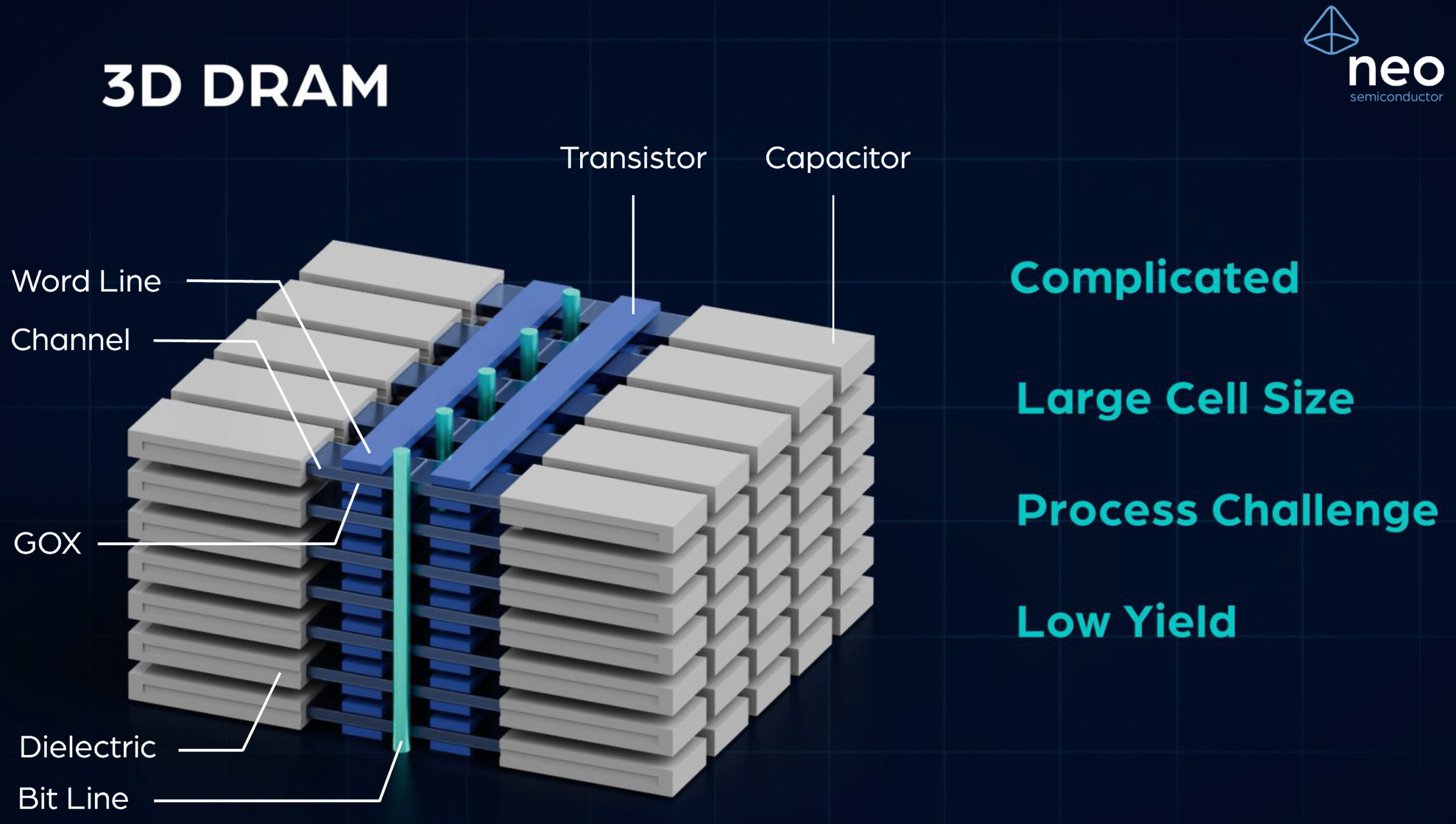
Traditional DRAM chips rely on a planar (2D) structure, typically composed of millions to billions of storage cells—each consisting of a capacitor and a transistor (1T1C)—laid out on a flat silicon substrate. Increasing cell density and performance has conventionally relied on shrinking the physical dimensions of devices, driven by advancing lithography nodes (down to sub-15nm feature sizes nowadays). However, the approach is increasingly constrained by several core challenges:
• Lithographic Scaling Limits: As feature sizes shrink below 20nm, physical and quantum effects (such as electron tunneling, gate leakage, and variability in material properties) make further scaling difficult and expensive.
• Capacitor Scaling Problem: Maintaining sufficient capacitance in ever-smaller cells is challenging. Thinner dielectrics and new materials (high-k dielectrics) help, but eventually capacitance and retention suffer.
• Increased Leakage and Refresh Rate: Higher leakage currents at smaller geometries lead to increased refresh cycles and power consumption, negatively impacting energy efficiency and long-term scaling prospects.
• Thermal Management: Greater density translates to increased power per unit area, complicating heat dissipation.
Despite innovations like HBM (High Bandwidth Memory), which leverages stacked dies with TSVs (Through Silicon Vias), these solutions present additional complexity and cost and rarely constitute true monolithic 3D integration.
3D DRAM: Pushing Past Planar Limits
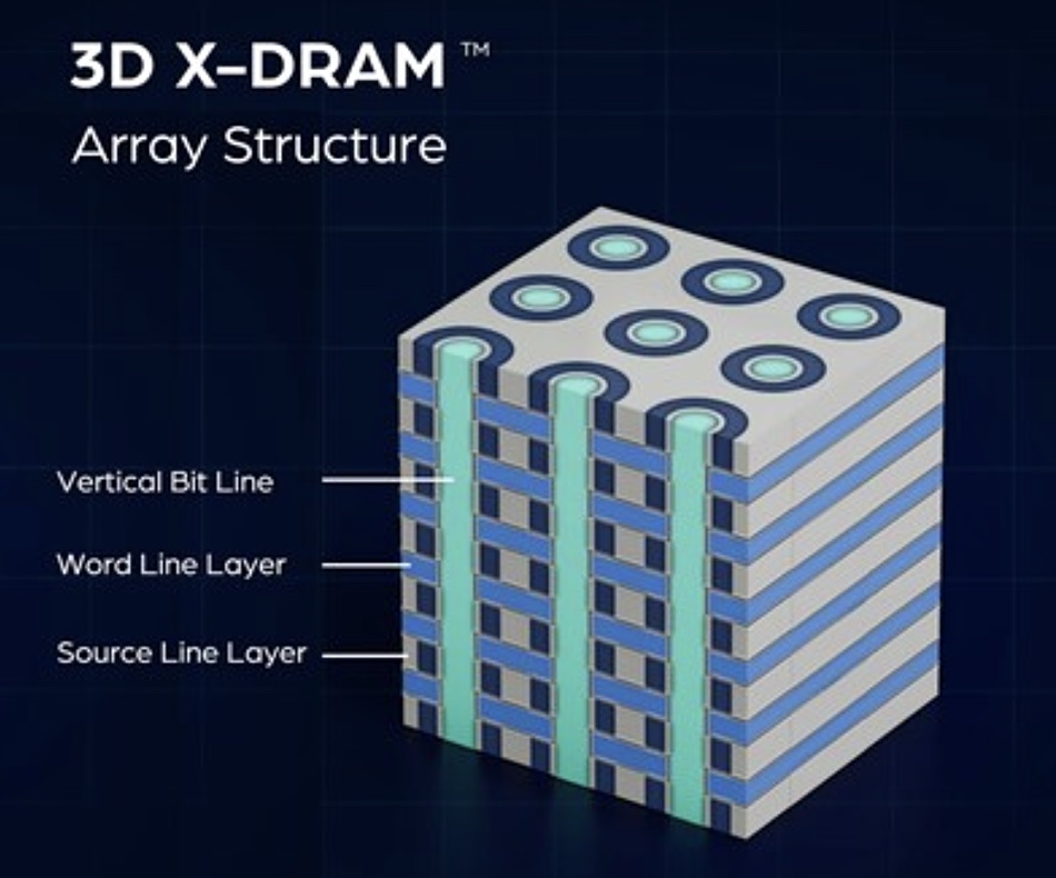
The recent breakthrough in 3D DRAM pivots on vertical stacking of multiple memory layers, fundamentally increasing memory density and bandwidth. This innovation, inspired by the success of 3D NAND, involves stacking active DRAM layers on top of each other and interconnecting them using TSVs, micro-bumps, or hybrid bonding.
Key Technical Features
• Monolithic Vertical Stacking: Multiple logic and memory device layers integrated within the same die, enabled by advanced epitaxial growth (e.g., Si/SiGe) and atomic layer deposition techniques. IMEC has demonstrated successful growth of up to 300 alternating silicon and silicon-germanium layers on 120mm wafers, opening the path for commercial-scale 3D DRAM.
• Next-Generation Cells: Novel cell architectures, such as capacitorless 3T0C (three transistor, zero capacitor) and IGZO (Indium Gallium Zinc Oxide) based structures, extend retention times and lower refresh energy budgets.
• TSV and Hybrid Bonding Interconnects: Through-silicon vias and wide-bus hybrid bonding give high-bandwidth access (e.g., up to 32K-bit wide data buses in new X-HBM 3D DRAM) and low-latency vertical communication across layers.
• Material Innovations: New dielectrics and channel materials (e.g., IGZO, high-k oxides) improve charge retention and reduce power loss, enabling scalability and manufacturability compatible with existing NAND processes.
• Thermal Management: Incorporation of advanced heat sinks and thermally aware chip stacking (e.g., dedicated thermal vias, optimized layer order) help mitigate the increased heat load from high-density vertical integration.
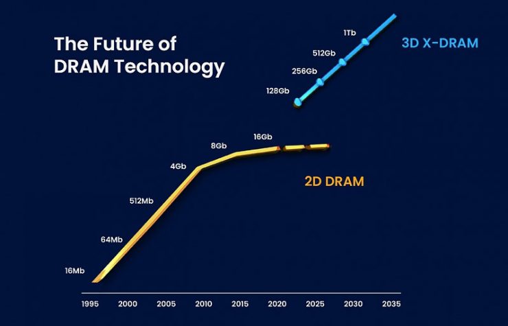
• Scalability: With vertical stacking, layer count can reach hundreds, enabling up to 8–16 times the bit density per chip over planar DRAM, with densities demonstrated up to 128Gb–512Gb/chip.
Vertical 3D DRAM architectures unlock several distinct advantages:
• Extreme Density: Increased cell layers boost bit density exponentially. NEO Semiconductor’s IGZO-based X-DRAM prototypes demonstrated 230–300 layers, with eightfold density gains over planar DRAM.
• Bandwidth and Latency: Short vertical interconnects between logic and memory, together with wide parallel bus architectures, achieve both high bandwidth and lower latency. The new X-HBM architecture, for example, pushes bandwidth up to 16x that of today’s DDR5 and HBM2.
• Power Efficiency: Reduced signal travel distances and retention-extension cell designs (e.g., 450-second retention times) slash power requirements for refresh. TCAD simulations verify ultra-low power operation while maintaining fast 10ns read/write speeds.
• Heterogeneous Integration: 3D stacking enables seamless integration of DRAM with logic, SRAM, flash, and custom accelerators in single packages, facilitating specialized AI and edge computing solutions.
• Scalable Manufacturing: Processes compatible with 3D NAND fabrication mean manufacturers can leverage existing equipment and yields, potentially reducing qualification hurdles.
Technical Challenges and Drawbacks
The march toward commercial 3D DRAM is not without hurdles:
• Manufacturing Complexity: Achieving uniform deposition, alignment, and etching across hundreds of stacked layers demands cutting-edge process control and 3D metrology tools.
• Yield and Scaling Risks: Early wafer and chip yields may be low as manufacturers adapt and optimize for high-layer-count vertical DRAM.
• Thermal Bottlenecks: Stacked structures concentrate heat. Management strategies require innovations in chip-level cooling (active cooling, thermal bonds, phase change materials).
• Cost: Upfront Fab investments, process development, and initial lower yields mean higher costs until volume ramps bring economies of scale.
• Ecosystem Updates: DRAM controllers, memory interfaces, and system architectures need new protocols to fully exploit bandwidth and integration benefits, requiring extensive R&D and ecosystem alignment.
• Reliability and Retention: Long-term reliability in new materials (e.g., IGZO) and novel cell designs must meet data-center grade lifetimes (5+ years), necessitating ongoing stress testing and refinement.
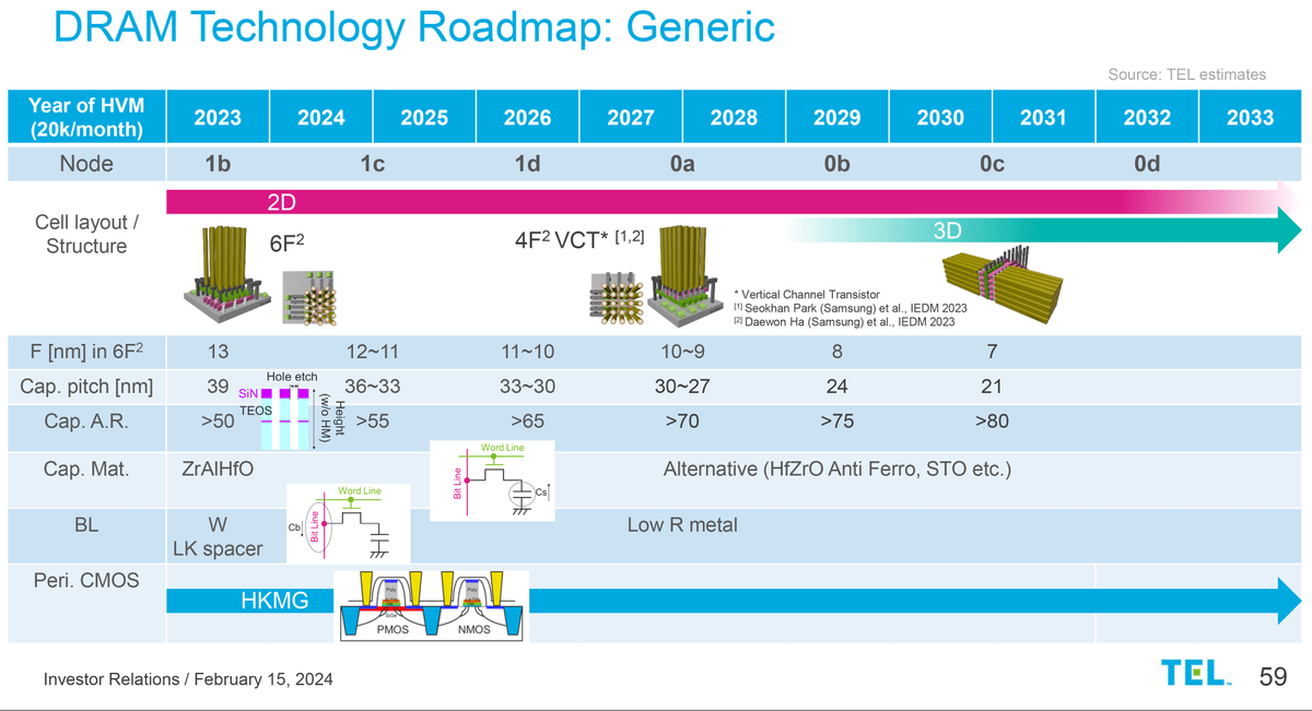
Industry Roadmap and Adoption Timeline
Industry projections suggest a multi-year transition path for 3D DRAM commercialization:
• Prototype and Early Production: First proof-of-concept chips with 1T1C, 3T0C, or NEO IGZO-based architectures expected in late 2026.
• Initial Markets: High-performance computing, cloud data centers, and enterprise AI accelerators are expected to lead early adoption, benefiting from the immediate density and bandwidth gains.
• Mainstream Adaptation: As costs fall and processes mature, mainstream applications—consumer electronics, smartphones, embedded systems—are forecast to begin integrating 3D DRAM within 4–5 years.
• Competitive Landscape: Major players (Samsung, Micron, NEO Semiconductor, BeSang) are investing heavily, with Asia-Pacific likely to dominate manufacturing due to infrastructure and demand from regional data centers.
• Yield and Cost Reduction: Ongoing advancements in process equipment, QC, and stack engineering will drive yields up and costs down mirroring the path that 3D TLC NAND flash took from niche to market dominance in less than a decade.
Summary & Adaptation Insights
The latest breakthroughs in 3D DRAM materials and vertical architectures represent a foundational advance in memory technology, overcoming long-standing performance, density, and energy bottlenecks of planar DRAM. Engineers will soon harness devices with over 300 active layers, IGZO and novel material platforms, and ultrawide data buses suited for next-gen AI and HPC. While manufacturing and reliability hurdles remain, the ecosystem is rapidly maturing.
Crucially, the rapid industry-wide adaptation of 3D TLC NAND—moving from pilot production to widespread market acceptance within a few technology cycles—offers a strong precedent for how quickly 3D DRAM may proliferate. TLC NAND’s journey showed that, once manufacturability hurdles and controller compatibility are managed, adoption curves accelerate sharply. We can reasonably expect 3D DRAM to follow a similar trajectory, especially as demand for bandwidth-hungry, efficient memory drives the market.
In summary, while technical, economic, and ecosystem challenges exist, electrical engineers and memory system designers should prepare now for a future shaped by 3D DRAM—where scalability, bandwidth, and integration open new possibilities across the computing spectrum.
E-mail: [email protected]
Tel: +972.77.540.1143