In-Cell CTP Technology: A Deep Technical Overview for Engineers Introduction
In-Cell Capacitive Touch Panel (CTP) technology represents one of the most complex integrations in modern display engineering. Unlike traditional touch modules—G/G (Glass-Glass), OGS (One-Glass-Solution), or On-Cell architectures—In-Cell embeds the X–Y touch electrodes directly within the TFT (Thin-Film Transistor) layer of the LCD or OLED stack.
Instead of adding a discrete touch sensor layer laminated above the display, In-Cell merges display pixel-driving circuits and mutual-capacitive touch detection circuitry within the same substrate. This reduces stack height, improves optical throughput, and changes the entire electrical architecture of touch sensing, particularly in noise-dominated environments.
Technology Architecture
1. Electrode Formation Inside the TFT Layer
In In-Cell designs, the touch electrodes are integrated on the same plane as one of the TFT layers:
LCD In-Cell
- Touch electrodes are formed on the array substrate, typically above the pixel electrodes but below the color filter.
- The electrodes often share routing layers with display lines (Gate/Source), requiring very tight electromagnetic compatibility (EMC) control.
OLED In-Cell
- Touch electrodes are patterned on the encapsulation (TFE) or integrated with the anode structure, depending on the AMOLED stack.
2. Mutual-Capacitive Touch Sensing
Most In-Cell designs use mutual capacitance due to the limited sensing area:
- TX electrodes send a high-frequency excitation signal.
- RX electrodes capture changes in mutual capacitance caused by a finger or conductive object.
- The “node capacitance” per intersection is typically 0.3–1.0 pF, much lower than in on-cell modules (3–10 pF), requiring advanced noise filtering.
3. Integrated Display Noise Management
The biggest engineering challenge: display noise generated by:
- Gate driver switching
- Source driver voltage transitions (15–20 V typically in a-Si LCD)
- Vcom flicker
- PWM backlight switching
- OLED pixel refresh current
Therefore, In-Cell systems use:
- High-order digital filters (FIR/IIR)
- Frequency hopping (10–300 kHz)
- Differential sensing
- Synchronous sampling aligned with blanking intervals
This co-design between touch IC and display driver (DDIC + TDDI) is what makes In-Cell solutions competitive.
TDDI: Touch + Display Driver Integration
Modern In-Cell screens rely heavily on TDDI (Touch and Display Driver Integration) ICs.
Engineering benefits:
- Shared timing control
- Coordinated noise suppression
- Lower power consumption (fewer ICs, fewer lines)
- Reduced BOM cost
- Better performance in wet-touch and glove-touch modes.
Engineering constraints:
- Limited customization for industrial or rugged devices
- Requires panel manufacturer + IC vendor collaboration early in design
- Higher NRE costs for custom sizes
Advantages (Engineering Level)
1. Structural & Optical
- Eliminates at least one glass/plastic layer → reduces reflections by ~4–8%
- Optical transmittance improvement of 3–10% depending on AR coatings
- Better luminance uniformity due to reduced air gaps
2. Form Factor
- Thickness reduction: 0.3–0.7 mm compared to On-Cell
- Weight savings up to 10–15 g on handheld devices
- Narrower bezels possible due to integrated routing
3. Electrical Performance
- Lower touch latency (5–15 ms typical)
- Better signal-to-noise ratio (SNR) in edge-area rejection
- Reduced parasitic capacitance compared to overlay sensor stacks
Disadvantages (Engineering-Level Detail)
1. Limited Ruggedization
Because electrodes are embedded inside the panel:
- Thick cover lenses (up to 6 mm) reduce touch sensitivity
- Wet-touch and gloved-touch performance depends heavily on TDDI tuning
- Industrial operability (EMI immunity >10 V/m) may require shielding films
2. Complex Manufacturing Processes
In-Cell production requires:
- Additional photolithography steps
- More precise TFT patterning tolerances
- Coordinated DDIC + TDDI tuning
- Calibration of touch electrode linearity in mass production
Yield drops significantly for:
- Larger sizes (>10 inches)
- High-resolution OLED In-Cell due to fine-pitch electrodes
- Harsh environments (sunlight-readable, high-brightness modules)
3. Repair Limitations
If a touch function fails:
- The entire display + electrode stack must be replaced
- No option to replace laminated touch glass like in G/G or OGS
Key Application Sectors
1. Consumer Electronics
- Smartphones, tablets, laptops
- High emphasis on form factor and optical clarity
- In-Cell is now the dominant technology in premium smartphones
2. Portable Medical Devices
- Low weight
- High optical performance
- Multi-touch with precise finger detection
3. IoT & Smart Home Products
- Sleek, compact enclosures
- Integration with low-power microcontrollers
4. Automotive Interiors
Used mainly for:
- Center stack displays
- Secondary infotainment screens
- Less common for primary HMIs requiring thick, laminated cover lenses or haptic overlays.
5. Industrial HMIs
Used selectively where:
- Touch precision matters
- Device depth must be minimized
Not ideal for extreme durability or glove-dominant usage.
Manufacturing Insight: When to Choose In-Cell vs. On-Cell vs. G/G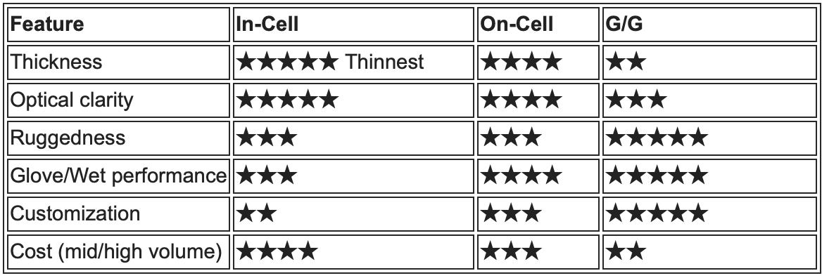
If your product requires:
- High brightness
- Thick cover glass
- Custom shapes
- Harsh EMC environments
Then On-Cell or G/G remains the better design choice.
Summary
In-Cell CTP technology offers clear engineering advantages—reduced thickness, improved optical performance, high touch accuracy, and TDDI-driven efficiency. It delivers a premium user experience, especially in handheld or compact devices where optical clarity and responsiveness dominate requirements.
However, engineers must account for:
- Noise suppression challenges
- Reduced ruggedization
- More complex manufacturing
- Lower customization flexibility
For high-volume consumer, medical, and slim industrial products, In-Cell remains one of the most effective touch architectures available today.
If you need support choosing the right display architecture, customizing touch performance, or sourcing In-Cell modules for your next design, contact me at: [email protected]
I’ll be glad to support your engineering and sourcing requirements.
E-mail: [email protected]
Tel: +972.77.540.1143